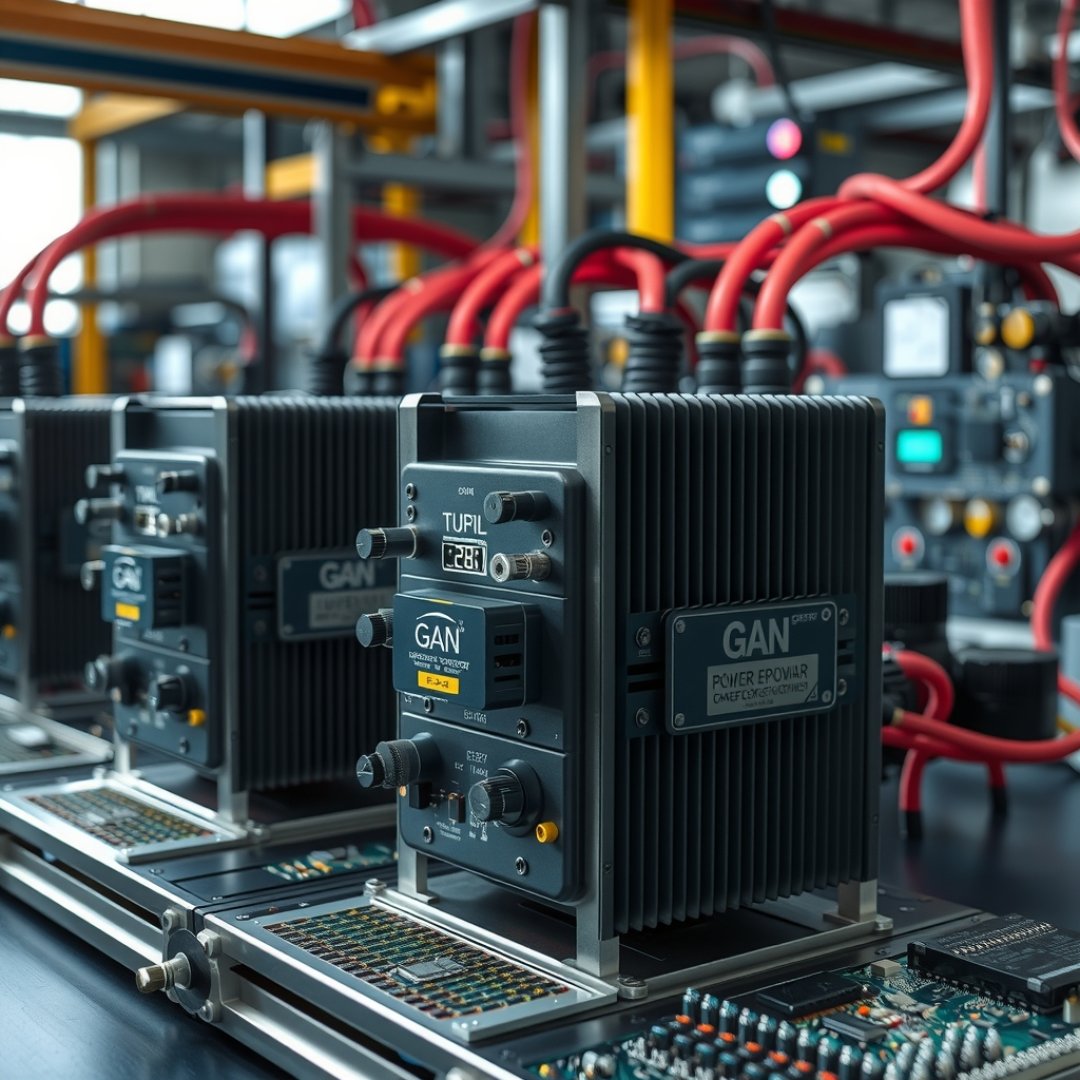
The integration of Gallium Nitride (GaN) into modern electrical infrastructure has fundamentally shifted the performance benchmarks for power electronics. As we navigate the technical requirements of 2026, GaN Power Converters have become the industry standard for high-voltage applications, offering superior electron mobility and faster switching speeds compared to traditional Silicon MOSFETs. By drastically reducing conduction and switching losses, these devices enable significantly higher power densities in compact grid-tied hardware. Engineering teams are increasingly adopting these wide bandgap materials to meet the rigorous thermal and efficiency demands of current smart energy grids and renewable energy storage systems, ensuring that power conversion architectures remain both compact and highly sustainable during peak operational loads.
Technical Advantages of GaN Over Silicon
Material Properties and Electron Mobility
Gallium Nitride possesses a significantly wider bandgap of 3.4 eV compared to Silicon’s 1.1 eV, allowing for higher breakdown voltages and operation at elevated temperatures. The inherent material properties of GaN facilitate a higher critical electric field, which enables the design of thinner drift layers for a given voltage rating.
- Lower Gate Charge: Reduces the energy required for switching cycles.
- High Electron Mobility: Enables ultra-fast switching frequencies in the MHz range.
- Reduced Parasitic Capacitance: Lowers switching losses, resulting in efficiency gains often exceeding 98% in hard-switching topologies.
Thermal Management and Power Density
Optimizing Heat Dissipation
Because GaN Power Converters minimize internal power dissipation, the reliance on massive heatsinks is substantially reduced. This shift toward high-density power conversion allows engineers to design smaller, lighter enclosures for residential and commercial battery energy storage systems (BESS).
Integration in Grid-Tied Applications
In 2026, the adoption of GaN in bidirectional grid-tied inverters has been pivotal. By operating at higher switching frequencies, these converters allow for the use of smaller passive components, such as inductors and capacitors, which lowers the overall CAPEX and environmental footprint of the hardware.
Compliance and Reliability Standards
Regulatory and Industry Benchmarks
Deployment of these converters must adhere to stringent industry protocols. IEEE 1547 standards for distributed energy resources (DER) integration are increasingly met by leveraging the precise control capabilities of GaN-based systems. Reliability testing, specifically focusing on dynamic on-resistance (RDS(on)) shifts, is critical for maintaining long-term grid stability.
- Testing for gate drive stability during high-frequency operation.
- Ensuring compliance with electromagnetic compatibility (EMC) regulations in dense urban grid environments.
- Verification of thermal cycling performance in harsh environmental conditions.
Frequently Asked Questions
What is the primary benefit of using GaN in power converters?
GaN provides higher electron mobility and a wider bandgap, allowing for much faster switching speeds and lower energy losses than silicon-based components.
How do GaN converters affect grid-tied inverter design?
They enable higher power density by allowing the use of smaller passive components, which reduces the physical footprint and material costs of the inverter.
Are GaN Power Converters suitable for high-voltage grid applications?
Yes, their material properties allow them to handle higher breakdown voltages, making them ideal for the evolving requirements of modern high-voltage smart grids.