
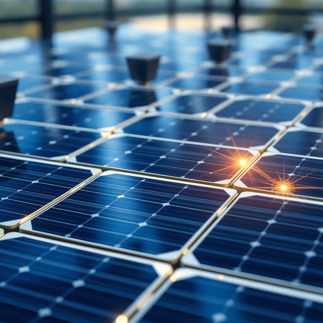
The integration of Perovskite-Silicon Tandem Cells into global utility-scale solar projects represents the most significant breakthrough in photovoltaic technology for 2026. By layering a perovskite thin-film atop a conventional crystalline silicon substrate, engineers have successfully unlocked the ability to capture higher energy photons that traditionally pass through single-junction silicon wafers. This architectural optimization pushes commercial module efficiencies beyond the Shockley-Queisser limit, with mass-produced tandem panels now consistently demonstrating 28% to 30% aperture area efficiency. As the industry pivots toward these multi-junction devices, the primary technical challenge remains the long-term chemical stability of the perovskite layer, specifically concerning thermal degradation and moisture sensitivity under extreme operating conditions. As we approach the end of 2026, manufacturing standards are evolving to incorporate advanced encapsulation techniques and molecular passivating agents that address ionic migration, ultimately aiming to achieve the 25-year lifespan required for utility-grade infrastructure investment and accelerated grid decarbonization.
Mechanisms of Tandem Junction Efficiency
Spectral Harvesting Optimization
Perovskite-Silicon Tandem Cells operate by utilizing a bandgap engineering strategy. The top perovskite layer is tuned to absorb high-energy (blue) photons, while the bottom silicon junction recovers the remaining infrared (red) spectrum. This reduces thermalization losses, which are inherent in single-junction silicon devices where excess photon energy is wasted as heat.
- Bandgap Tunability: Perovskites allow for precise bandgap adjustments by altering halide compositions.
- Voltage Boost: The stacking of junctions effectively increases the open-circuit voltage (Voc) of the total module.
- Current Matching: Engineers utilize interconnecting tunnel junctions to ensure current density remains consistent across both layers, minimizing resistive losses.
Degradation Mitigation and Encapsulation Standards
Addressing Environmental Volatility
To meet the rigorous durability requirements defined by IEC 61215, manufacturers are implementing robust multi-layer barrier systems. These layers protect the perovskite against atmospheric moisture and oxygen, which historically initiated rapid decomposition.
Key Stability Improvements:
- Atomic Layer Deposition (ALD): Utilized to create ultra-dense diffusion barriers.
- Molecular Passivation: Incorporation of organic cations to mend surface defects and prevent ion migration under high irradiance.
- Edge Sealing: Use of advanced thermoplastic polyolefin (TPO) sheets to prevent moisture ingress at the panel perimeter.
Economic Implications and CAPEX Analysis
Scaling Commercial Manufacturing
The capital expenditure (CAPEX) for producing Perovskite-Silicon Tandem Cells has reached parity with premium n-type TOPCon modules. While the initial investment in tandem-specific production lines—including precision chemical vapor deposition—is higher, the LCOE (Levelized Cost of Energy) is significantly lowered due to the increased power density.
- Reduced Balance of System (BoS) Costs: Because tandem modules generate more power per square meter, the total footprint for land, racking, and wiring is reduced by approximately 15%.
- Energy Yield ROI: Higher conversion efficiency translates to improved performance ratios in low-light and high-temperature environments.
- Scalability: Industry leaders are leveraging existing silicon lines to perform the final integration, minimizing transition costs.
Frequently Asked Questions
What is the typical efficiency range for 2026 commercial tandem modules?
Current high-performance tandem modules demonstrate aperture area efficiencies between 28% and 30%.
Do Perovskite-Silicon Tandem Cells require different racking hardware?
No, they are compatible with standard racking systems, but their higher power density allows for a smaller mounting footprint.
How do manufacturers handle the degradation of the perovskite material?
Manufacturers use advanced encapsulation, atomic layer deposition for moisture barriers, and surface passivation to stabilize the perovskite layer.